
Application guide

Semiconductor And Electronic Materials

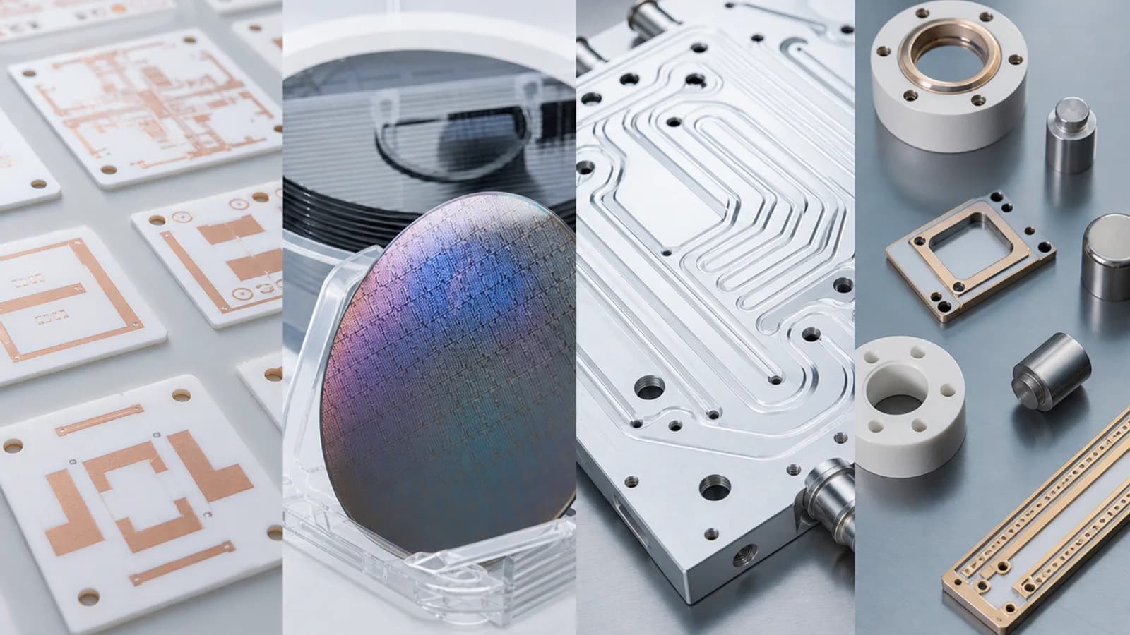
Electronics and packaging oriented thermal routes for electronic ceramics, targets, refractory metal parts, and precision joining assemblies — distinct from upstream semiconductor powder or substrate material preparation.

Semiconductor And Electronic Materials process

Process context

Material challenges and process focus

Semiconductor and electronics projects often require clean thermal environments, controlled atmosphere, repeatable recipes, and traceable process records. Equipment configuration is reviewed around material purity, thermal profile, joint design, gas handling, and the inspection plan for the final component.

Typical Materials

Electronic ceramicsSputtering targetsRefractory metalsPackaging assembliesPower-device components

Recommended Equipment

Vacuum FurnaceDiffusion Bonding FurnaceSPS Sintering System

Process Focus

Clean sinteringElectronic ceramic densificationHermetic packaging

Application FAQ

Which equipment is usually considered for Semiconductor And Electronic Materials?

Vacuum Furnace, Diffusion Bonding Furnace, SPS Sintering System

What process information should be prepared before inquiry?

Material, target temperature, atmosphere, pressure or load, workpiece size, expected capacity, and project timeline.

Can Haoyue customize a furnace around this application?

Yes. Chamber size, heating zone, pressure system, gas control, fixtures, and automation can be reviewed according to the process requirement.